LibreCube Board Specification
This page provides the normative specification of LibreCube boards. These boards are used in stacked configuration and typically contain system components or entire subsystems (for example, a power system) or larger sensors and actuators. All LibreCube board projects must follow this specification.
The reason for defining such a board specification is to enforce a consistent and modular design of LibreCube elements. Much of this specification is inspired by the typical design of CubeSat boards, which however was never formally defined. This is quite a paradox because the success of the CubeSat program is clearly due to its standardized form factor. The internal electronic boards were never specified by the CubeSat program, which has led to many incompatible CubeSat boards, even among vendors. This shows that it is extremely important to define a formal specification of such boards.
You may want to use the template board as starting point for your board development.
Mechanical Specification
The shape and dimensions of the board are shown below. The origin is placed in the bottom left corner.
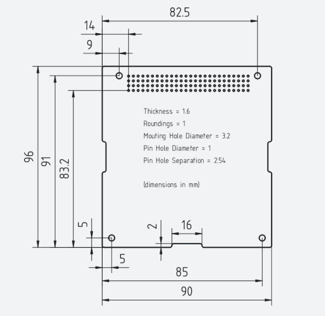
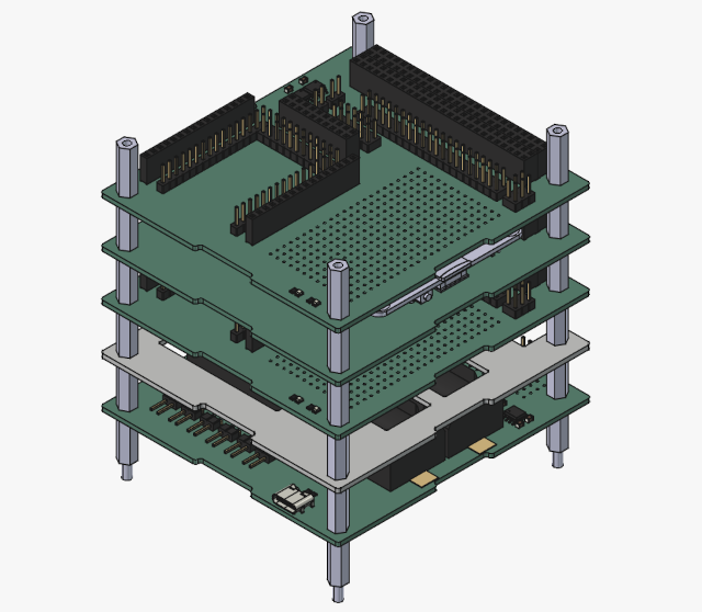
Boards can be stacked on top of each other. Spacing between boards is 16 mm. The preferred side to mount components is the top side. Components should not exceed a height of 8.5 mm above the top side. Components should not exceed a height of 4.5 mm below the bottom side.
Electrical Specification
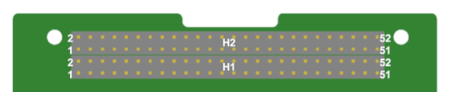
The naming of the headers (H1 and H2) and the pin numbering is:
The allocation of the pins of the two headers is as shown below.
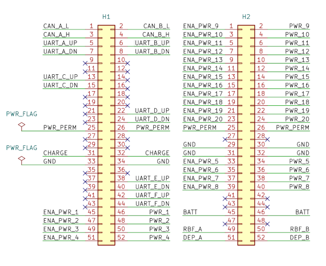
Connector H1
| Pin | Name | Description |
|---|---|---|
| 1 | CAN_A_L | CAN Bus A Low Line (1 MBps) |
| 2 | CAN_B_L | CAN Bus B Low Line (1 MBps) |
| 3 | CAN_A_H | CAN Bus A High Line (1 MBps) |
| 4 | CAN_B_H | CAN Bus B High Line (1 MBps) |
| 5 | UART_A_UP | TM/TC Bus A Uplink (115200 baud) |
| 6 | UART_B_UP | TM/TC Bus B Uplink (115200 baud) |
| 7 | UART_A_DN | TM/TC Bus A Downlink (115200 baud) |
| 8 | UART_B_DN | TM/TC Bus B Downlink (115200 baud) |
| 13 | UART_C_UP | TM/TC Bus C Uplink (115200 baud) |
| 15 | UART_C_DN | TM/TC Bus C Downlink (115200 baud) |
| 22 | UART_D_UP | TM/TC Bus D Uplink (115200 baud) |
| 24 | UART_D_DN | TM/TC Bus D Downlink (115200 baud) |
| 25 | PWR_PERM | Permanent 5V Output |
| 26 | PWR_PERM | Permanent 5V Output |
| 31 | CHARGE | Battery Charge Input (2.5 - 5.5 Volt) |
| 32 | CHARGE | Battery Charge Input (2.5 - 5.5 Volt) |
| 33 | GND | Ground |
| 34 | GND | Ground |
| 38 | UART_E_UP | Payload Bus E Uplink (115200 baud) |
| 40 | UART_E_DN | Payload Bus F Downlink (115200 baud) |
| 42 | UART_F_UP | Payload Bus F Uplink (115200 baud) |
| 44 | UART_F_DN | Payload Bus F Downlink (115200 baud) |
| 45 | ENA_PWR_1 | Enable Power Line 1 |
| 46 | PWR_1 | Power Line 1 Output (5 Volt) |
| 47 | ENA_PWR_2 | Enable Power Line 2 |
| 48 | PWR_2 | Power Line 2 Output (5 Volt) |
| 49 | ENA_PWR_3 | Enable Power Line 3 |
| 50 | PWR_3 | Power Line 3 Output (5 Volt) |
| 51 | ENA_PWR_4 | Enable Power Line 4 |
| 52 | PWR_4 | Power Line 4 Output (5 Volt) |
Connector H2
| Pin | Name | Description |
|---|---|---|
| 1 | ENA_PWR_9 | Enable Power Line 9 |
| 2 | PWR_9 | Power Line 9 Output (5 Volt) |
| 3 | ENA_PWR_10 | Enable Power Line 10 |
| 4 | PWR_10 | Power Line 10 Output (5 Volt) |
| 5 | ENA_PWR_11 | Enable Power Line 11 |
| 6 | PWR_11 | Power Line 11 Output (5 Volt) |
| 7 | ENA_PWR_12 | Enable Power Line 12 |
| 8 | PWR_12 | Power Line 12 Output (5 Volt) |
| 9 | ENA_PWR_13 | Enable Power Line 13 |
| 10 | PWR_13 | Power Line 13 Output (5 Volt) |
| 11 | ENA_PWR_14 | Enable Power Line 14 |
| 12 | PWR_14 | Power Line 14 Output (5 Volt) |
| 13 | ENA_PWR_15 | Enable Power Line 15 |
| 14 | PWR_15 | Power Line 15 Output (5 Volt) |
| 15 | ENA_PWR_16 | Enable Power Line 16 |
| 16 | PWR_16 | Power Line 16 Output (5 Volt) |
| 17 | ENA_PWR_17 | Enable Power Line 17 |
| 18 | PWR_17 | Power Line 17 Output (5 Volt) |
| 19 | ENA_PWR_18 | Enable Power Line 18 |
| 20 | PWR_18 | Power Line 18 Output (5 Volt) |
| 21 | ENA_PWR_19 | Enable Power Line 19 |
| 22 | PWR_19 | Power Line 19 Output (5 Volt) |
| 23 | ENA_PWR_20 | Enable Power Line 20 |
| 24 | PWR_20 | Power Line 20 Output (5 Volt) |
| 25 | PWR_PERM | Permanent 5V Output |
| 26 | PWR_PERM | Permanent 5V Output |
| 29 | GND | Ground |
| 30 | GND | Ground |
| 31 | GND | Ground |
| 32 | GND | Ground |
| 33 | ENA_PWR_5 | Enable Power Line 5 |
| 34 | PWR_5 | Power Line 5 Output (5 Volt) |
| 35 | ENA_PWR_6 | Enable Power Line 6 |
| 36 | PWR_6 | Power Line 6 Output (5 Volt) |
| 37 | ENA_PWR_7 | Enable Power Line 7 |
| 38 | PWR_7 | Power Line 7 Output (5 Volt) |
| 39 | ENA_PWR_8 | Enable Power Line 8 |
| 40 | PWR_8 | Power Line 8 Output (5 Volt) |
| 45 | BATT | Direct Battery Output (2.5 - 4.2 Volt) |
| 46 | BATT | Direct Battery Output (2.5 - 4.2 Volt) |
| 49 | RBF_A | Remove Before Flight |
| 50 | RBF_B | Remove Before Flight |
| 51 | DS_A | Deployment Switch |
| 52 | DS_B | Deployment Switch |
The power enable lines are CMOS logic level.
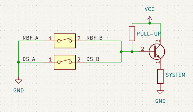
The Remove Before Flight pin shall un-power the system when fitted. The Deployment Switches shall un-power the system when both of the switches are pressed. The figure below exemplifies this logic.
The switchable power lines can be used for switching subsystems and equipment. The permanent 5V lines shall power the essential equipment to allow commanding at all times. All other units are switchable and may use redundancy; in that case they are powered through either nominal or redundant power line. If redundancy is not used, then either of the two lines may power the unit. It is up to the system design how to define this switchable lines. A recommended usage is given here:
- PWR_PERM: Permanent line, for reconfiguration board and communications receivers
- PWR 1/2: Power board interface
- PWR 3/4: Communications board interface
- PWR 5/6: Computer A and B
- PWR 7/8: Thermal board interface
- PWR 9/10: Navigation board interface
- PWR 11/12: Propulsion board interface
- PWR 13/14: Motion board interface
- PWR 15/16: Mechanism
- PWR 17/18: Payload board interface
- PWR 19/20: (mission-specific)
References